Delta Driver Addressing
The Delta Driver supports both Delta style addressing (such as D0 or X0.0) or standard 6-digit Modbus addressing (4XXXXX). Note that this differs from the VTScada Modbus Compatible driver, which supports both 5 and 6 digit addressing.
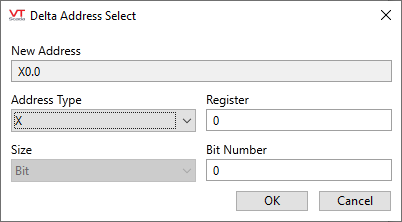
I/O tags using the Delta Driver provide access to an Address Select dialog, which supports Delta style addressing based on the Hardware Type selected.
You can read strings from register-based addresses in PLCs such as Delta and Modbus by setting the "String stored in registers" flag of the IO tag, along with specifying the length in bytes. See: I/O Tab, String data type layout
Addressing Prefixes
| P | Parameter |
| CR | Control Command |
| SR | Status Monitor Read Only |
| OD | Option Device Information |
| RI | Remote IO |
| SD | String Display Description |
| ID | Internal General Definition |
Address Types
The following table outlines the types of addresses available for each Hardware type and the type of data held in the address. To access the output bit of Timers (T) and Counter (C, HC), add ".0" to denote that data type instead of the value of the Timer or Counter.
In the format column, "D" denotes "decimal. "O" denotes "octal".
|
AS | AH | DVP 3 | DVP | |||||||
|---|---|---|---|---|---|---|---|---|---|---|---|
| Format | Range | Format | Range | Format | Range | Format | Range | ||||
| X | Bit | DD.DD | X0.0~X63.15 | DD.DD | X0.0~X1023.15 | OOO | X0~X377 | OOO | X000~X377 | ||
| Word | DD | X0~X63 | DD | X0~X1023 | - | - | - | - | |||
| Y | Bit | DD.DD | Y0.0~Y63.15 | DD.DD | Y0.0~Y1023.15 | OOO | Y0~Y377 | OOO | Y000~Y377 | ||
| Word | DD | Y0~Y63 | DD | Y0~Y1023 | - | - | - | - | |||
| M | Bit | DDDD | M0~M8191 | DDDD | M0~M8191 | DDDD | M0~M8191 | DDDD | M0~M8191 | ||
| D | Bit | DDDDD.DD | D0~D32767.15 | DDDDD.DD | D0~D1048575.15 | N/A | N/A | ||||
| Word | DDDDD | D0~D32767 | DDDDD | D0~D1048575 | DDDDD | D0~D32767 | DDDDD | D0~D11999 | |||
| S | Bit | DDDD | S0~S2047 | DDDD | S0~S2047 | DDDD | S0~S2047 | DDDD | S0~S1023 | ||
| T | Bit | DDD | T0.0~T511.0 | DDD | T0.0~T2047.0 | DDD | T0.0~T511.0 | DDD | T0.0~T255.0 | ||
| Word | T0~T511 | T0~T2047 | T0~T511 | T0~T255 | |||||||
| C | Bit | DDD | C0.0~C511.0 | DDD | C0.0~C2047.0 | DDD | C0.0~C511.0 | DDD | C0.0~C199.0 | ||
| Word | C0~C511 | C0~C2047 | C0~C511 | C0~C199 | |||||||
| Bit | - | - | - | - | - | - | DDD | C200.0~C255.0 | |||
| DWord | - | - | - | - | - | - | C200~C255 | ||||
| HC | Bit | DDD | HC0.0~HC255.0 | DDD | HC0.0~HC63.0 | DDD | HC0.0~HC255.0 | - | - | ||
| DWord | HC0~HC255 | HC0~HC63 | HC0~HC255 | - | - | ||||||
| SM | Bit | DDDD | SM0~SM4095 | DDDD | SM0~SM4095 | DDDD | SM0~SM4095 | - | - | ||
| SR | Word | DDDD | SR0~SR4095 | DDDD | SR0~SR4905 | DDDD | SR0~SR2047 | - | - | ||
| E | Word | D | E0~E9 | D | E0~E31 | D | E0~E9 | - | - | ||
Delta AX Series PLC addressing using Modbus
The addressing assumes that the default offsets of 0 for MW, 256 for QW, and 0 for IW are set in DIA-Designer. If the offsets are adjusted, the VTScada addresses will need to differ from the PLC addresses to account for the change. As an example, given a PLC that has a QW offset of 300 for registers, then %QW0 on the PLC would be equivalent to %QW44 due to the change in offset.
Digital addressing:
Takes the form of MXI.J, where I is an offset in Bytes, and J is the offset in bits from the Byte offset. For example, if an address of MX0.3 is provided, the Modbus coil would be 100004. If an address of MX2.2 is provided the coil value is 100019.
